Arbitrary Code Execution on a GameBoy with Pokémon Yellow
tl;dr: I ran homebrew Pong on a GameBoy by using a normal Pokémon Yellow cartridge like a flashcart.
Introduction
I’d been aware of glitches in first-gen Pokémon games for a while now, but recently I wanted to see the limits of what they could do. Turns out that besides super fast speedruns, you can also use these glitches to run almost any code. The catch is that these hacks require suitable emulators since they might use thousands of inputs per frame to write the payload code they’ll execute. This means that repeating them on a GameBoy probably isn’t possible. The glitches used to trigger these exploits work the same on the hardware though. So if we could store a payload in a cartridge we could run it, essentially treating a normal cartridge as if it were a flashcart. In this post I’ll go through how I did just that by modifying the data saved in RAM in a Pokémon Yellow cartridge to run a homebrew version of Pong.
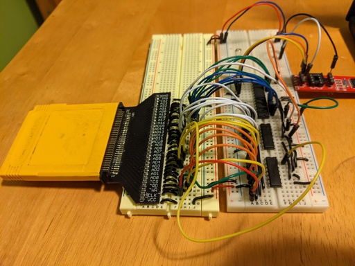
The convenient thing about the setup, shown above, is that very little specialized hardware is needed. The only GameBoy-specific things required are an english Pokémon Yellow cartridge and a cartridge breakout board like the one used here. I used that same board which can be ordered off OSHPark. I also used a microcontroller and a couple of shift registers to make things easier. More specifically, I ended up using an ATmega328P and SN74HC595s. The choice of microcontroller doesn’t really matter too much, but the use of shift registers did turn out to be more important than I initially thought. Later on I’ll point out things to consider when choosing these parts.
Using Pokémon Yellow was an easy choice since the data layout of the cartridge’s 32KB of RAM is well-documented, not to mention it’s the only GameBoy cartridge that I own with RAM. So the idea here is to use the breakout board and microcontroller to write custom save data to the cartridge’s RAM, then trigger an in-game glitch to run homebrew code embedded in the save data. Before breaking out any hardware though, it’d be good to test this idea in an emulator to see if it’ll actually work. So how do we actually make use of an exploit to run homebrew?
Exploiting the game
Out of the many known exploits in Yellow, I chose to go with the ws m glitch. To enable this glitch we just modify Bag Items to get one ws m item. Its effect pointer is documented as 0xDA7F. That means that when the item is used in-game, the console’s program counter will point to that address. This tells the console to start running code from that address. To make sense of the address let’s take a look at the gameboy’s memory-map.
  0x0000-0x3FFF   16KB ROM Bank 00     (in cartridge, fixed at bank 00)
  0x4000-0x7FFF   16KB ROM Bank 01..NN (in cartridge, switchable bank number)
  0x8000-0x9FFF   8KB Video RAM (VRAM) (switchable bank 0-1 in CGB Mode)
  0xA000-0xBFFF   8KB External RAM     (in cartridge, switchable bank, if any)
  0xC000-0xCFFF   4KB Work RAM Bank 0 (WRAM)
  0xD000-0xDFFF   4KB Work RAM Bank 1 (WRAM)  (switchable bank 1-7 in CGB Mode)
  0xE000-0xFDFF   Same as C000-DDFF (ECHO)    (typically not used)
  0xFE00-0xFE9F   Sprite Attribute Table (OAM)
  0xFEA0-0xFEFF   Not Usable
  0xFF00-0xFF7F   I/O Ports
  0xFF80-0xFFFE   High RAM (HRAM)
  0xFFFF          Interrupt Enable Register
External RAM at 0xA000-0xBFFF is used for the cartridge’s RAM, which is split up into four 8KB banks that can be individually mapped to this section. The address 0xDA7F, however, falls within a 4KB work RAM bank inside the console. Not ideal, but we can make it work.
While our idea doesn’t allow us to directly write to work RAM, this table shows that the game copies parts of the cartridge’s save data there. More specifically, the last byte of Main Data is copied to 0xDA7F followed by Current Box Data starting at 0xDA80. This means that the data copied from these locations will get interpreted as code and executed when we use the glitch item. However, Current Box Data is only 1122 bytes which limits the amount of code we can execute this way. As a workaround we could put the payload at the start of another RAM bank and only put a bit of code in Current Box Data to swap banks and trampoline to 0xA000. This would give us a whole 8KB to work with. Also keep in mind that although we’ll put our trampoline code in cartridge RAM, it’ll be executed from the copy in internal work RAM. This means that we can swap RAM banks and keep running this bit of code without issue. That then raises the question, what external RAM bank would we prefer?
To pick a RAM bank for storing the payload, we should consider how the game validates its save data. Yellow does this by computing checksums and deleting the saved game if invalid data is detected. While we will have to recalculate the checksum for the bank with the trampoline, it turns out that bank 0 isn’t validated, allowing us to store the payload there. To recap, the plan so far is:
- Modify
Bag Itemsat0x5C9in bank 1 to get onews mglitch item - Put a trampoline in
Current Box Dataat0x10C0in bank 1 - Fix the bank 1 checksum
- Put the payload in bank 0
- Use
ws min-game to run the payload
Getting the glitch item
With the plan ready, let’s open up Yellow in an emulator, create a new game then save the game when we get a chance. As soon as we open up Yellow, the emulator should create a .sav file. This contains external RAM data, which we can verify is 32KB. Now let’s open up the .sav in a hex editor to take a look. Here I opened up the file in vim then used the :%!xxd command to get a readable hexdump of the binary file. The first step is modify Bag Items to get one glitch item so let’s navigate to 0x25C9, which will probably look like this
000025C0: 0000 0000 0000 0000 0000 FF00 0000 0000 ................
The layout of Bag Items starts with the number of items, followed by the entry IDs and is terminated with 0xFF. So let’s add one ws m (item ID 0x63) by changing the line to
000025C0: 0000 0000 0000 0000 0001 63FF 0000 0000 ................
Let’s also note that we added a net total of 0x01 + 0x63 = 0x64 to the bank’s save data for when we have to fix the checksum. The next step is then to make the trampoline, so let’s navigate to 0x30C0.
Making the trampoline
To make the trampoline we’ll have to write assembly, translate it to hex using the instruction set encoding then write it to Current Box Data at 0x30C0. Note that the last byte of Main Data gets copied from 0x2D2B to 0xDA7F and will also be interpreted as code. However, it’s zero which is a nop, so let’s leave it as is and put the whole trampoline in Current Box Data for simplicity. Now the very first thing the trampoline should do is disable interrupts to ensure we only run our code. Then it enables the cartridge’s RAM and swaps in bank 0, resets the stack pointer and jumps to the beginning of the payload. This is mostly straightforward with the exception of bank swapping and enabling RAM. That part is cartridge-specific and in this case Yellow handles those operations with a memory bank controller (MBC5). When any program tries writing a valid bank number anywhere in the read-only address range 0x4000-0x5FFF, the specified bank is swapped in by the MBC5. Similarly when a program tries writing certain values in the range 0x0000-0x1FFF RAM is enabled or disabled. Putting everything together, the trampoline at 0x30C0 might look something like this
  30C0:    F3             di             ; disable interrupts
  30C1:    21 00 00       ld $hl, 0x0000 ; load address to enable RAM
  30C4:    36 0A          ld (hl), 0x0A  ; enable RAM
  30C1:    21 00 40       ld $hl, 0x4000 ; load address to swap banks
  30C4:    36 00          ld (hl), 0x00  ; swap in bank 0
  30C6:    31 FE FF       ld $sp, 0xFFFE ; reset the stack pointer
  30C9:    C3 20 A0       jp 0xA020      ; start homebrew program
Here we changed the start of the payload from 0xA000 to 0xA020 because testing showed that the game overwrites the first 32 bytes of bank 0 on startup. Now let’s write this to the .sav with our hex editor again
000030C0: F321 0000 360A 2100 4036 0031 FEFF C320  ................
000030D0: A000 0000 0000 0000 0000 0000 0000 0000  ................
and note the net change to the save data. Including the previous +0x64 and a -0xFF removed from 0x30C1, the net total checksum change so far is +0x501.
Fixing the checksum
To fix the checksum let’s navigate to 0x3523. In my case it was originally 0xB7, though each new game randomizes things so it’ll probably differ. To recalculate it subtract the old checksum from the net change, then the new value will be 0x100 minus that difference mod 0x100. In this case the new checksum would be 0x100 - ((0x501 - 0xB7) % 0x100) = 0xB6. So this line
00003520: 0000 00B7 FFFF FFFF FFFF FFFF FFFF FFFF ................
becomes
00003520: 0000 00B6 FFFF FFFF FFFF FFFF FFFF FFFF ................
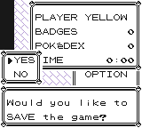
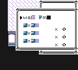
We can then save our hexdump as a binary using the vim command :%!xxd -r > new_file.sav and open up our emulator with this new .sav. We should now have one ws m item, meaning we’re on the right track.
Assembling the payload
Finally we get to the interesting part of deciding what payload to run. While we do have nearly 8KB available, it won’t be as easy as just putting a normal game in the .sav. The program has to either use position-independent code or take into account that it’s running from RAM instead of ROM if it uses absolute addresses. In this case I decided to go with a Pong demo I had previously written since it could easily be reassembled to run from different addresses. To get it to work from RAM I had to modify my assembler by setting startAddress and mainAddress to 0xA020 and 0xA023, respectively, then removing the line truncating file size. Then I just recompiled Pong with the new assembler.
To store this in the save data we just open the resulting GameBoy executable in a hex editor, then copy rows 0xA020-0xA2F0 from pong.gb to rows 0x0020-0x02F0 of the .sav and fix the addresses on the left-hand side. With the .sav complete we can save the hexdump as a binary again and reload the emulator. Now using the ws m item like so
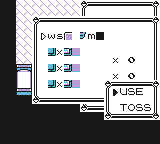
allows us to play the Pong program embedded in the save data. Aside from some graphical glitchs and the backdrop, it behaves just like the standalone Pong demo.
Executing code on the GameBoy
With our idea verified by an emulator, let’s now consider how to run it on the GameBoy. Although there are plenty of demonstrations of the reading/writing with cartridges and its timing diagrams, the first hardware tests should be as simple as possible. A good first step might be to just modify Bag Items to get a ws m item. After ensuring we have the item in-game, we can write the trampoline and final payload to the cartridge. Before the first test though, let’s review the process of writing to the physical cartridge’s RAM.
Writing to RAM is almost identical to changing the .sav file. The main difference is that instead of addressing the 32KB of RAM as one continuous slice, we need to use the MBC5 and 8KB address range 0xA000-0xBFFF. This means keeping in mind which RAM bank the MBC5 has mapped to that range. Another consequence of using a physical cartridge is that we must first enable/disable the RAM to prevent data loss. With those differences in mind, we’re now ready to do the first write tests.
Testing cartridge writes
When we modified the .sav to get the ws m item, we had to read from memory to update the checksum in addition to writing. Since we want to keep our first tests simple, we’d like to stick with just writing and avoid reading for now. We can do this by ensuring that the net change to the cartridge data is zero (or any multiple of 0x100) to avoid having to change the checksum. Recall that we obtained the ws m item by changing the following addresses from
  25C9:    00
  25CA:    FF    ; terminates the list of items
  25CB:    00
to
  25C9:    01    ; item count
  25CA:    63    ; ID of glitch item
  25CB:    FF    ; terminates the list of items
It turns out that terminating the list with 0xFF isn’t actually necessary if the item count is non-zero. So we can change 0x25CA to 0x63 to get the item just like before, then make the item count 0xFF - 0x63 = 0x9C to keep the net change at zero. That section then becomes
  25C9:    9C    ; increased item count
  25CA:    63    ; ID of glitch item
  25CB:    00    ; removed list terminator
This way we can get the glitch item and simultaneously satisfy the checksum without reading. Although we’re only writing to two addresses, enabling/disabling RAM and swapping in RAM bank 1 also are treated as writes. This means that we need to do a total of five writes in the following order
0x0Aat0x0000to enable RAM0x01at0x4000to load RAM bank 10x63at0x25CAto get the glitch item0x9Cat0x25C9to increase the item count and satisfy the checksum0x00at0x0000to disable RAM
To follow the process used for the .sav more closely, let’s first start and save a new game with the physical cartridge. With that ready, let’s look at how to wire things up.
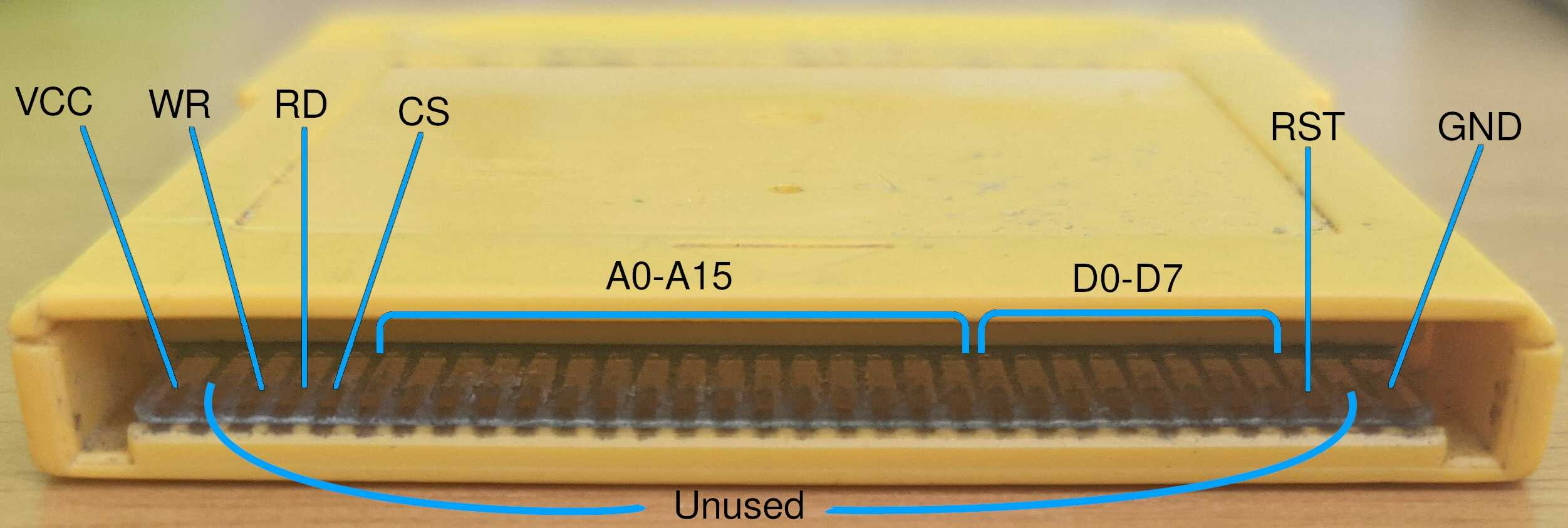
The cartridge has 32 pins with the pinout labels on the image below. Going from left to right and ignoring the unused pins next to VCC and GND we have
- VCC: 5V input power source
- WR: write select
- RD: read select
- CS: SRAM select
- A0-A15: 16 input address pins with the least-significant bit (LSB) on the left
- D0-D7: 8 input/output data pins with the LSB on the left
- RST: reset
- GND: ground
Due to the large number of address and data pins, I originally tried using a 40-pin ATmega324P to drive the cartridge. This significantly simplified the wiring since each cartridge pin could be directly connected to an I/O pin on the microcontroller. However, tests showed that I couldn’t drive the cartridge this way. Trying to read various addresses made the cartridge output ~3.6V on random subsets of the data pins even though the cartridge was running on 5V. From the voltage droop on the microcontroller’s high output pins and plots of the chip’s pin driver strength, I very roughly estimated that the cartridge was pulling ~5 mA on these pins. This isn’t a problem for any individual pin, but the ATmega324P is limited to sourcing 100 mA in total from all its pins. Because of this limit a buffer is needed to drive the cartridge. In this case serial-in/parallel-out 74HC595 shift registers are the ideal choice since they have the required drive strength and additionally simplify the microcontroller-side wiring. With the reduced need for I/O pins, I decided to use a 28-pin ATmega328P.
Since each shift register has only 8 outputs, I daisy-chained two of them to drive the 16 address pins as shown below. Each shift register’s outputs drive one byte of the address pins with the QAs corresponding to the LSBs.
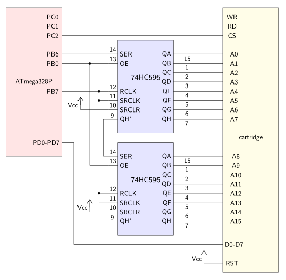
The remaining cartridge pins, with the exception of RST, were just connected directly to the ATmega328P. The pins WR, RD, CS and RST all use negative logic, meaning they are active when pulled low, which is why RST is tied to VCC. At this point, we’re ready to look at the code for driving the cartridge and shift registers.
The ATmega code, which is partly shown below, is mostly self-explanatory. After initializing pins as inputs or outputs with the DDRB, DDRC and DDRD registers, we can call the functions below to shift out values to the shift registers and write values to the cartridge.
#define SR_OE (1 << PB0)
#define SR_DATA (1 << PB6)
#define SR_CLK (1 << PB7)

// Shifts a 16-bit `value` into the shift registers and enables their output.
void shift_out(uint16_t value) {
    // This disables the output since OE uses negative logic
    PORTB |= SR_OE;
    for (int i = 0; i < 16; i++) {
        // Iterate through bits starting from the LSB
        uint8_t bit = (value >> i) & 1;
        if (bit == 0) {
            PORTB &= ~SR_DATA;
        } else {
            PORTB |= SR_DATA;
        }
        PORTB |= SR_CLK;
        PORTB &= ~SR_CLK;
    }
    // Re-enable the output
    PORTB &= ~SR_OE;
}
In the write function we introduce an arbitrary 20 ms delay after setting WR low to give the cartridge ample time to process the write. This is likely a far longer delay than is actually needed, but there doesn’t seem to be any timeout so it’s fine.
#define DELAY 20
#define ROM_SIZE ((uint16_t)0x8000)
#define GB_WR (1 << PC0)
#define GB_RD (1 << PC1)
#define GB_CS (1 << PC2)

void write(uint16_t addr, uint8_t value) {
    // Disables these functions since they use negative logic
    PORTC |= GB_WR | GB_RD | GB_CS;
    // Set the address pins
    shift_out(addr);
    // Sets the data pins
    PORTD = value;
    // Enable `CS` if we're writing outside ROM
    if (addr >= ROM_SIZE) {
        PORTC &= ~GB_CS;
    }
    // Toggle `WR` with a long delay
    PORTC &= ~GB_WR;
    _delay_ms(DELAY);
    // Reset pins to their default
    PORTC |= GB_WR;
    if (addr >= ROM_SIZE) {
        PORTC |= GB_CS;
    }
}
With these basic functions we can now do the first write test to get the glitch item with the microcontroller. This should take almost no time to complete, but I connected an LED to the microcontroller to ensure the process had ended.
Now we see the glitch item in-game, as expected.
Writing the payload to RAM
At this point we’ve shown that writing to cartridge RAM works and we’re ready to put in the trampoline and write the payload. To convert the payload to a readable format, we can use the command xxd -i pong.sav > ace_sav.h and remove the irrelevant parts of the header file. Then for the trampoline it’ll be easiest to keep the same assembly code shown above and just recalculate the checksum manually. For this calculation we’ll need to be able to read from memory though.
The read function below closely mirrors the write function above except that PORTD should be configured as all inputs in this case. Again we give the cartridge ample time to process the read and show the correct value on the data pins by introducing a 20 ms delay.
uint8_t read(uint16_t addr) {
    PORTC |= GB_WR | GB_RD | GB_CS;
    shift_out(addr);
    if (addr >= ROM_SIZE) {
        PORTC &= ~GB_CS;
    }
    // Toggle `RD` with a longer delay
    PORTC &= ~GB_RD;
    _delay_ms(DELAY);
    // Read data pins
    uint8_t value = PIND;
    PORTC |= GB_RD;
    if (addr >= ROM_SIZE) {
        PORTC |= GB_CS;
    }
    return value;
}
After swapping in and modifying bank 1, we can simply recalculate the checksum as follows
#define WRITE_ALL ((uint8_t)0xFF)
#define READ_ALL ((uint8_t)0)

#define RAM_OFFSET ((uint16_t)0xA000)
#define CHECKSUM_START ((uint16_t)0x598)
#define CHECKSUM_OFFSET ((uint16_t)0x1523)

DDRD = READ_ALL;
uint8_t checksum = 255;
for (uint16_t i = CHECKSUM_START; i < CHECKSUM_OFFSET; i++) {
    checksum -= read(RAM_OFFSET + i);
}
DDRD = WRITE_ALL;
write(RAM_OFFSET + CHECKSUM_OFFSET, checksum);
This manual recalculation simplifies the process since we don’t have to track what values we overwrite in each section, but it does noticeably increase the time required to patch the cartridge. This only takes about a minute and a half, but like before we can just use an LED to ensure the process finished. Putting it all together as shown here and writing to the cartridge again now allows us to trigger the exploit in-game to play Pong on the GameBoy.
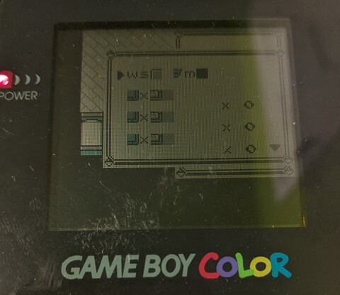
Here we initially see some new graphical glitches, but after a few rounds they fade and we get the same behavior seen on the emulator.
Conclusion
So we’ve seen it’s possible to abuse glitches in Yellow to run homebrew on a GameBoy without a flashcart. What more could we possibly want at this point? Well one thing we didn’t consider was using this process to patch Yellow itself. That could work by using the glitch as an in-game trigger to write to specific locations in RAM, similar to how a gameshark works. For example the well-known gameshark code 010138CD allows you to walk through walls in Yellow. It does this by writing 0x01 to address 0xCD38 which we can replicate by replacing our trampoline with the following code.
  30C0:    F5             push $af       ; save the game's registers
  30C1:    E5             push $hl
  30C2:    21 38 CD       ld $hl, 0xCD38 ; load the address to modify
  30C5:    7E             ld $a, (hl)    ; read the address
  30C6:    EE 01          xor $a, 0x01   ; toggle the LSB
  30C8:    77             ld (hl), $a    ; overwrite the address
  30C9:    E1             pop $hl        ; load the game's registers
  30CA:    F1             pop $af
  30CB:    C9             ret            ; return to the game
In this case instead of setting 0xCD38 to 0x01, we can xor its value with 0x01 to allow us to toggle the hack on and off. After writing this to the cartridge as shown here, we can now toggle walk through walls in-game.
While all this was interesting, we could do a lot more with this glitch. For starters, we didn’t even make use of the whole 32KB of RAM. Using the other RAM banks would’ve meant dealing with bank swapping and working around checksums, but it’s definitely possible if we needed more memory. Another thing we could’ve looked into was using the cartridge’s ROM in our homebrew program. For examples, this could mean reusing the graphics data in ROM. In Pong this would’ve saved 72 bytes or nearly 10% of the payload size. Also there exist disassembly projects and Ghidra supports the GameBoy so reusing Yellow’s code in a homebrew program is even a possibility. Really all of this is just scratching the surface of what’s possible.